Terafab's 1 Million Wafer Target Leaves Its Memory Plans Open
Terafab's reported post-2032 target of 1 million wafers a month would rival Samsung's DRAM output, but its memory process and partners remain undisclosed.
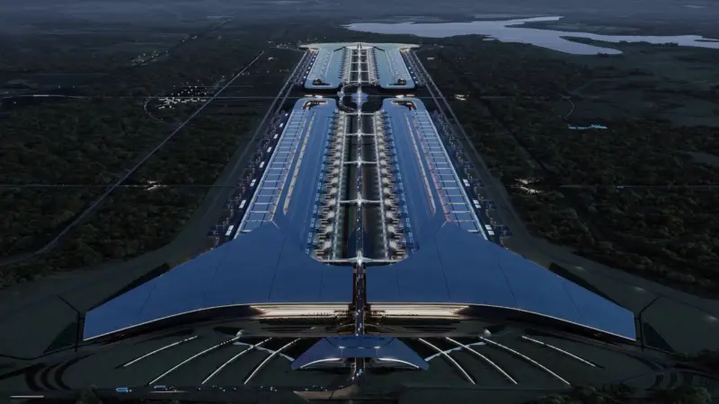
The number itself is the headline. Terafab, the joint venture of Tesla and SpaceX, has told equipment makers informally that it wants to produce 1 million wafers per month after 2032, according to Financial News. What makes the figure hard to dismiss is how it's split. About 70%, or 700,000 wafers, is earmarked for memory, and more than 300,000 for logic. Even if the target slips by years, the scale of the intent tells you this isn't a side project.
What 700,000 memory wafers actually compares to
Here's the thing: the comparison to Samsung is tempting, and it needs care. Samsung's DRAM capacity was estimated last year at 650,000 to 700,000 wafers a month. SK hynix is reportedly near 550,000, with a goal of about 1 million by 2030. Terafab's memory allotment would sit at or above the largest of those figures.
But that's apples and oranges. Terafab's 700,000 covers all of its expected memory output, which could be NAND or DRAM. The Samsung and SK hynix numbers measure DRAM only. So the honest reading is that Terafab's memory target is a total-capacity figure that, if it were all DRAM, would rival the biggest DRAM producers in the world. For scale, the memory portion alone would be 3.5 times the reported 200,000 wafers at SK hynix's Wuxi fab in China.
The memory question is the real gap
Memory is where the plan gets murky. Memory production generally splits between DRAM and NAND flash, and the two are built very differently. Terafab hasn't said which it intends to make, and it's not clear what type of memory is on the docket.
The hiring record offers some clues without settling the question. A Tesla job listing for a Terafab Memory Process Integration Engineer, reported in August, covers end-to-end DRAM process integration and DRAM node development. It also references emerging memories such as MRAM, RRAM, and 3D DRAM. That points toward DRAM-centric work, but it doesn't confirm a production plan.
Product mix is another open question. Terafab's job postings mention both HBM and LPDDR, two DRAM families that matter a lot for AI workloads. The company hasn't said how its output would divide between them, or whether it expects to fabricate and stack the DRAM itself or package chips it sources elsewhere. Those choices change the economics, the tooling and the customer base, so they're worth watching. Technical help from a Taiwanese company is under consideration for memory, but no partner has been named. That leaves 70% of the planned wafers without a disclosed process technology.
Logic is further along, at least on paper
On the logic side, Jiji Press reports that Terafab is working with Intel to adopt its 2nm and 1.4nm processes. That gives the logic portion a more concrete technical anchor than the memory portion has. Building a leading-edge logic fab on U.S. soil is still a hard problem, though, and Tesla and SpaceX don't have chip-manufacturing experience. Teams in this position usually find that process recipes are the easy part to describe and the hardest part to get yielding at volume.
A tight schedule that its own leader calls aggressive
The timeline is the part most people in the industry are skeptical about, and Musk has been upfront about that. On a SpaceX call last month, he called Terafab's dates "very aggressive" and said he put "big error bars" on the timeline. The company is targeting volume production in the second half of 2028. Planning to volume at a leading-edge fab typically takes three years or more, so that target compresses a long path.
Early milestones are more modest and more checkable. The first SRAM test chip is targeted for around May or June 2027 at the Austin research facility. A pilot plant could be completed as early as July 2027. Those dates are the ones to track, because they show whether the schedule is holding before the volume targets come into play.
Supply-chain activity is already moving. Terafab's procurement team visited Japan to ask local toolmakers for delivery within months, and some suppliers were asked to deliver within a few months of the request. Representatives also visited the booths of about 10 Korean materials, parts, and equipment firms at SEMICON West, with some NDAs signed, according to The Elec. Orders like these are why the plan is being taken more seriously now than it was when Musk first announced it in March, even if the final scope is still unclear.
TSMC, money and what comes next
How TSMC fits in remains open. TSMC has said any fab with its involvement would have to be run by TSMC. Musk has said his own companies would build and operate Terafab. Those positions don't obviously reconcile, and the more likely near-term outcome is one where TSMC's role stays limited.
The spending plans are at least defined. The first phase is $16.8 billion in Grimes County, Texas, with total investment of up to $119 billion if later phases proceed.
My read is that the number of wafers is the least informative part of this announcement. The more useful signals over the next year are which memory type Terafab commits to, whether it names a process partner, and whether the 2027 test chip and pilot plant arrive on schedule. Until those are answered, the 1 million wafer figure describes an ambition more than a production plan.