Staera Bets on Light Inside the Chip With $4.6M Pre-Seed Round
Staera's $4.6M pre-seed round funds Lightwire, an on-chip optical interconnect it says could replace copper links between AI accelerator chiplets.
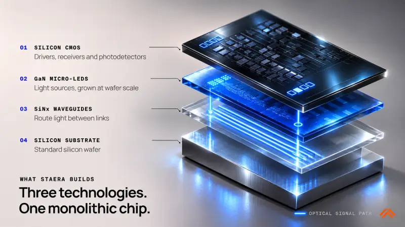
Staera Semiconductor, a San Francisco startup building technology to link chiplets together, has launched with $4.6 million in pre-seed funding. The amount is small by chip-industry standards, but the problem it targets is real. The wiring that stitches a high-end AI accelerator together is becoming a limiting factor, and Staera wants to replace the copper in that wiring with light.
Where copper runs out
Modern AI accelerators aren't single slabs of silicon. They're assembled from multiple chiplets, each one a separate die handling a narrow set of tasks. Those dies communicate through a small network that also serves as the base layer of the accelerator package. That network usually takes one of two forms: an interposer, which is an advanced substrate that can sometimes carry computing circuits of its own, or a bridge, which is essentially a smaller interposer that's cheaper to make.
Both rely on tiny copper wires to move data between chiplets. Copper does the job at short range, but the distances that matter most in AI accelerators run from millimeters to meters, and that's where Staera argues copper falls behind. CEO Andrew Kim framed the problem directly: "Copper performance plummets over the millimeter-to-meter distances that matter most in AI accelerators, and bolt-on optics add power and complexity."
Kim's pitch is about where the optics sit. Rather than attaching external optical modules to the package, Staera wants the optical link built inside the chip. In his words, "We build the light into the chip, the entire optical link inside a chip, so the connection gets smaller, cooler and faster with each generation." That's a design choice with real consequences. Pluggable or co-packaged optics add physical interfaces and extra conversion steps, and each of those costs power. Integrating the link removes some of that overhead, at the cost of pushing the manufacturing challenge onto the chip itself.
How Lightwire is built
Staera's first product, Lightwire, carries data over optical waveguides made from silicon nitride, a transparent material. Light can only propagate through a transparent medium when its wavelength falls within a particular range, so the choice of material matters. According to Staera, silicon nitride supports a wider range of wavelengths than many alternatives and loses less light along the way. Less loss means a cleaner signal and, in the company's framing, higher connection speeds.
The light itself comes from miniature LEDs made of gallium nitride. That compound is widely used in optical devices because it has a direct bandgap. Here's the physics in plain terms: when an electron drops from a higher energy band and recombines with a hole, it releases a photon. In indirect-bandgap materials, that process usually needs a phonon, a lattice vibration, to conserve momentum. Direct-bandgap materials like gallium nitride skip that requirement, so light generation is more efficient. For a chip-scale design where every milliwatt counts, that efficiency is the reason the material choice makes sense.
The numbers Staera is putting forward
Staera says Lightwire transmits data between an AI accelerator's chiplets at rates of up to 8 gigabits per second and can support more than 600 optical links per square millimeter. The most striking claim is about memory. The company says a Lightwire-equipped HBM4 memory stack could move up to 24 terabits of data per second, compared with 2.8 terabits per second for current technologies. That would be roughly eight and a half times the bandwidth.
These are the company's own figures, and the article doesn't include independent measurements, test configurations or a comparison against rival optical approaches. Still, the direction is clear. Memory bandwidth has become one of the main constraints on AI hardware, and an interconnect that scales in density and speed without a power penalty would address a real pain point. The open question is how the 8 Gbps link rate and the 24 Tbps stack figure relate to each other in an actual system, since aggregate bandwidth depends heavily on how many links run in parallel.
Money, timeline and what comes next
The round was led by Singaporean fund Openspace Capital. It was joined by SGInnovate, Black Kite Capital, 28 Holdings, In Group and financial software company Decimus Technologies. Staera plans to use the funding to commercialize its technology: enhancing Lightwire, growing its U.S. team and building out a manufacturing supply chain. The company hopes to begin commercial shipments in 2030.
That timeline is long, and it tells you something about the work ahead. Integrating optical waveguides and light sources into a chip means dealing with materials, packaging, thermal behavior and yield, and each step depends on suppliers that don't yet have mature processes for this kind of integration. Teams in this position typically spend a long stretch proving out prototypes before the supply chain can support volume. Staera's 2030 target suggests it expects that path to take years rather than quarters.
My read: the core idea, building the optical link into the chip, addresses a problem the industry will keep running into as accelerators grow. Whether Lightwire can deliver on its numbers at production scale is the question that matters. Watch for reported measurements on real silicon, details on how the gallium nitride LEDs are integrated with silicon nitride waveguides, and the first design partners willing to put the technology into an accelerator package.