Faster Simulation and Digital Twins Are Changing How Fabs Test Process Changes
Accelerated simulation, physics-based AI and digital twins let fab engineers test more process changes before they touch the production line.
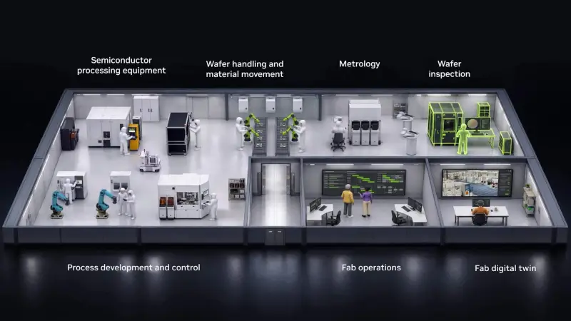
The most useful AI work in chip fabs isn't the chatbot-style tooling people tend to picture. It's the compression of analysis time. When evaluating a process change takes days, and a physical trial on a production line is slow and expensive, an engineer can only test a handful of ideas. Shorten the loop and that number grows.
That's the premise behind what NVIDIA and several equipment and software vendors are calling the AI-defined fab. The pitch is that AI helps engineers optimize processes, catch problems earlier and make better decisions, while they keep control of the calls. The speedups being reported are specific enough to examine, and they fall into three categories that are at different stages of maturity.
Shorter simulation cycles widen the search
Multiphysics simulations model how heat transfer, electrical behavior and mechanical stress interact, and those coupled problems are expensive to solve repeatedly. Using NVIDIA's cuDSS library, COMSOL is accelerating these simulations for semiconductor manufacturing by up to 10x. The practical effect is that engineers can compare more equipment and process alternatives in-house, then choose which few changes deserve a physical test.
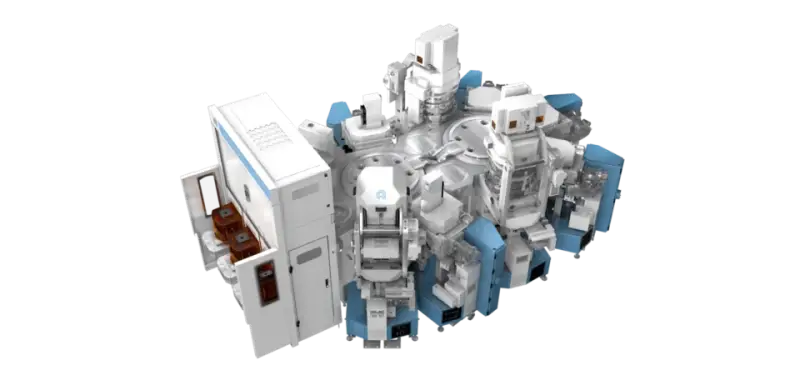
Applied Materials and NVIDIA are working on atomic-scale materials discovery and process development. With cuDSS integrated, Applied's Ginestra simulation platform runs up to 10x faster than CPU-only approaches. Applied's ACE+ multiphysics platform, paired with NVIDIA PhysicsNeMo, delivers topography simulations up to 35x faster. Topography matters here because surface shape after deposition and etch steps feeds directly into yield, so faster topography runs let teams check more variants before committing wafers.
Lithography is the more striking case. Computational lithography determines how circuit patterns are printed onto silicon, and the calculations involved are heavy enough that, at production scale, they can't practically finish on CPUs. That makes acceleration an enabler rather than a convenience. Siemens is integrating NVIDIA cuLitho into its Calibre lithography software, with up to 17x acceleration on key simulation workloads. That widens the set of patterns an engineer can verify before a wafer goes to print.
Faster calculation also helps researchers explore material behavior and reaction pathways, the groundwork for next-generation processes. That work is earlier-stage than production verification, but it's where a 10x difference in turnaround changes which questions people bother asking.
Predicting process behavior without running every simulation
Acceleration speeds up a solver. Physics-informed AI goes a step further by learning to predict outputs directly, so teams don't need a full simulation for every condition. The payoff is most visible in calculations that remain expensive even on accelerated hardware.
Plasma is a good example. Plasmas are the electrically charged gases used in etch, and modeling them means solving coupled electrical, chemical and thermal equations that interact in ways that make repeated runs costly. NVIDIA says PhysicsNeMo can reduce plasma-prediction simulation time from days to as little as milliseconds. That's the difference between checking a condition and sweeping a whole operating window.
Lam Research plans to integrate NanoVDB into SEMulator3D, its advanced process modeling platform within the Semiverse Solutions family of virtual products. The company expects that to accelerate select wafer-etch modeling by up to 30x. Here's the thing about figures like these: they describe speed on specific workloads, not across a fab's whole modeling stack. The real question for any team adopting a surrogate model is how closely its predictions track full physics runs across the conditions they actually care about, and how that gets validated and re-validated as tools age or recipes change.
Agents take over the steps between decisions
Engineers spend much of their time converting analyses into decisions: revising a design, chasing a test failure, adjusting a production process. Between those decisions sits a lot of procedural work, and that's where agents are starting to fit.
Choosing which AI model suits a given task is a useful illustration. Done by hand, it's a sequential process that can eat hours on the test floor. Advantest is using NVIDIA NeMo Switchyard AI agents to automate that selection, cutting response times from hours to minutes. The gain is less about any single model's accuracy and more about removing wait time from a routine decision, which matters when a test floor is waiting on the answer.
Agents of this kind are generally most reliable where the steps are well defined and the outputs are checkable. Teams in this position typically keep a human reviewing consequential choices, especially when an agent's recommendation would change a production setting rather than a planning step.
Testing factory changes before they reach the line
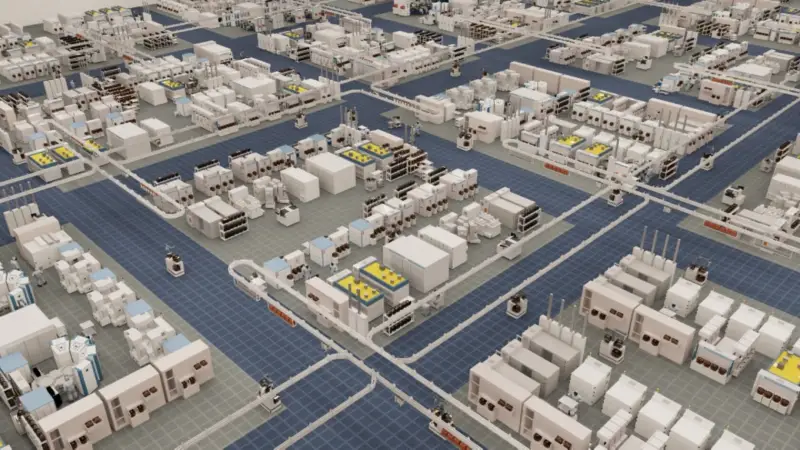
Digital twins extend simulation from a single process to the whole facility. Teams can model equipment configurations, layouts and process changes in a virtual environment before running physical trials. That lowers experimentation costs, and the value grows as fabs get more complex and a wrong change becomes more expensive.
Applied Materials uses NVIDIA Omniverse libraries to build physically accurate digital twins of entire fabs. Teams can simulate material movement, find bottlenecks, and evaluate layouts and operating strategies. Bottlenecks in material flow are often invisible in per-tool metrics, so a facility-level model can surface problems that process simulations never reach.
Where the loop gets hard
Most of the reported gains are measured on individual workloads, and the open engineering questions sit in the seams. Surrogate models need validation against physics-based results. Digital twins only stay useful if they're kept in sync with the real line, which requires clean production data flowing back in. And agents need clear boundaries around what they can change. None of these problems are unique to semiconductors, but fab tolerances make them unforgiving.
The connected loop
The more interesting future is the one where these pieces connect. Production data informs the models, the models evaluate changes, and the findings return to the engineers making decisions on the line. That's the loop the AI-defined fab describes: a cycle where teams learn from each production run and act on that knowledge sooner.
My read is that the near-term winners will be the fabs that get the validation and data plumbing right first, because a 30x faster model is only as useful as the trust engineers place in its answers.